Enhances Precision in Semiconductor Manufacturing through Laser Marking, Dicing, and Scribing by Laser Photonics and CMS Lasers
In the realm of industrial laser processing, Laser Photonics Corporation and its subsidiary, CMS Laser, stand as pioneers, offering cutting-edge technology for sustainable surface preparation, rust removal, corrosion control, de-painting, and more.
With a reputation for quality and innovation, Laser Photonics is a leader in the field, providing sophisticated laser machines equipped with proprietary software controls. CMS Laser, a 40-year U.S. pioneer in software controls development for laser machines, is at the forefront of this success.
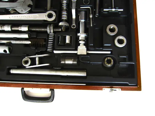
CMS Laser specialises in developing laser systems for a wide range of industries, tailoring its solutions to each client's unique manufacturing needs. In the semiconductor industry, the company offers turnkey laser material processing systems for marking, cutting, drilling, welding, cleaning, and more.
High-precision laser marking, dicing, and scribing capabilities are key features of CMS Laser's solutions for the semiconductor industry. These systems offer micro-level accuracy to create crisp, legible, and machine-readable markings such as data matrix codes and serial numbers, essential for traceability and quality control.
Unparalleled precision and efficiency are enabled by advanced gantry laser systems with dynamic three-axis motion platforms that handle diverse semiconductor part sizes and complexities without physical contact, reducing damage risk during processing.
Versatility allows configurations for cutting, drilling, welding, marking, dicing, and scribing, catering to a full spectrum of semiconductor manufacturing needs. Integrated machine vision streamlines alignment, validation, and quality control, improving throughput and reliability in high-volume production.
Durability and permanence of laser markings ensure reliable traceability throughout semiconductor component life cycles, as these markings resist fading, corrosion, abrasion, and other environmental factors. Non-contact processing prevents mechanical damage such as micro cracks or deformation, thereby preserving the structural and functional integrity of delicate semiconductor parts.
Sustainability and low maintenance benefits stem from minimal waste generation and reduced need for consumables like inks or chemicals, aligning with environmentally friendly manufacturing goals. CMS Laser's solutions also support advanced manufacturing technologies that leverage increased tax credits for U.S.-based chipmakers, positioning them as modern tools to enhance competitiveness and innovation in semiconductor fabrication.
Laser Photonics' new generation of laser blasting technologies addresses health, safety, environmental, and regulatory challenges associated with outdated surface processing methods. The CleanTech laser cleaning brand aims to disrupt the sand and abrasive blasting markets, offering a more sustainable and efficient alternative.
World's top manufacturers, including Fortune 1000 companies in various industries, rely on Laser Photonics' laser equipment to optimise their operations. CMS Laser counts several top 20 global life sciences companies among their customers and invites clients in the semiconductor industry to visit its Applications Lab and take advantage of its research area with a free sample evaluation.
Together, these features position CMS Laser’s solutions as robust, precise, and efficient tools that improve yield, quality, and sustainability in semiconductor manufacturing.
Read also:
- Important Characteristics to Consider when Choosing a Manufacturing Material
- The essentials of Sheet Metal and the Varieties That Exist.
- Optimum ERP Systems for Medium-Sized Enterprises in 2025: A Ranking of the Most Effective Solutions
- Record-Setting Start for MyCabin in New Year: Revenue Surges Over Twofold


